

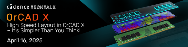
High Speed Layout in OrCAD X – It’s Simpler Than You Think!
Designing a high-speed PCB layout requires accuracy, attention to detail, and an understanding of signal integrity. Create more reliable designs by properly managing key signals to minimize noise, reduce crosstalk, and optimize performance. Whether you are an experienced designer looking to refine your techniques or a beginner just starting on your first high-speed design, there is something here for you.
You will learn about:
- Fundamentals of high-speed signals
- Key factors that affect the performance of high-speed signals
- How to utilize OrCAD X and Constraint Manager features for high-speed routing
- How to leverage In-Design Analysis for post-layout simulation and verification
Live attendees will gain access to the demo PCB database featuring common interfaces such as DDR3, HDMI, and more to explore all the topics covered during the session.
Unable to attend live? Register anyway and we will send you the recording so you can watch it at your convenience.
Clicking the link will redirect you to Cadence’s registration page